|
|
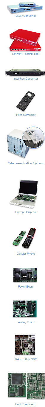
Gallery
We contribute to the Electronic Industry of tomorrow with our quality PCBs based on solid technology and diverse ideas.
System Development
üĪ Hardware Development capability
| üyDesign specüz |
Research of Technical Trend,
Value Analysis Recommendation
(Cost/Lead-time/Quality), Test Method Suggestion. |
| üySchematic Designüz |
Image Processing Engine Platform.
Multiple Memory System. |
| üy ā╩P üz |
H8, SH series, ARM, PQćV, TEGRA
MPC series, etc |
| üyFPGAüz |
ALTERA Stratix series.
Cyclone series.
XILINX Vertex series.
Spartan series.
Kintex series.
|
| üyAnalogüz |
A/D, D/A, Filter |
üĪ Software Development capability
| üyā╩P softwareüz |
C, VB, Assembler |
| üyIP Technologyüz |
IP, UDP, TCP, HTTP, TELNET |
| üyCommunication Technologyüz |
Specified Low Power Radio Station.
WiFi, NFC, Bluetooth. |
üĪ Equipment
OrCAD capture, Protel, System-Designer
Altera-MAX+PlusII, QuartusII, Xillinx-ISE, Design-Gateway
OEM/EMS
üĪ Case Design(Architectural Design/Mock Design)
| üyPlate metalüz |
Sheet metal processing, metal cutting, Tooling and Molding |
| üyresinüz |
Rapid prototyping(Stereolithography, Laser Sintering, Fused Deposition),
Rapid Prototype Tooling(silicon-type, aluminum-type),Tooling and Molding |
| üyFinishingüz |
face plate, painting, plating, alumite treatment |
üĪ Component Procurement, üĪ Assembly and Wiring
üĪ EMC/Safety Certificate Acquisition,Vibration/Aging/Reliability Test.
üĪ Support service, üĪ Translation and Documentation
üĪ Equipment
üyDesign/2Düz
|
AutoCADüiLT2006üj |
| üyDesign/3Düz |
Pro/ENGINEERüiWILDFIREüj |
| üyetc.üz |
Temperature and Humidity chamber, Electric measuring instrument. |
PCB Design
üĪ PCB Design capability
PCI-EXPRESS, HDMI, SATA, MIPI, 4K2K DDR3 SDRAM, Optical Module Device.
Audio/Video Device, High-speed switching Device.
High-Voltage 400V, High-Current 30A, RF 5.8GHz.
üĪ Schematic Design
üĪ Transmission Line Analysis Reflection analysis
1.Overshootü@ü@ü@2.Undershoot 3.Ringing backü@ü@4.Non Monotonic Crosstalk analysis, Clock wave analysis
üĪ EMI Simulation
EMI-DRC, Resonants Analysis
üĪ Equipment
| üyAnalysisüz |
MENTOR ICX, DEMITASNX |
| üySchematic Designüz |
ZUKEN Design Gateway, OrCAD Capture, Protel, ZUKEN System/Designer
DG(Design-Gateway) |
| üyPCB Designüz |
CADENCE Allegro, SPECCTRA Router
ZUKEN Board/Designe |
| üyCAM Editüz |
VALOR Enterprise, ORBOTECH Genesis,ORBOTECH InCAM |
Fabrication
üĪ Fabrication capability
| üyClassüz |
Single/Double side, MLB, High-MLB(68 layers), Stacked build up, SVH-board, Rigid Flexible |
| üySpecüz |
Minimum Line/Space : 50/50ā╩éŹ
Minimum VIA diameter : ā│0.1(Mechanical)
Layer count : 2layersü`68layers
Thickness : éöüü0.2ü`6.5mm
Board size : 600ü~500mm
Impedance control : 28āČü}10%, 50āČü}5%
Aspect ratio : 21
Power board : 175ā╩m cupper foil |
| üyMaterialüz |
FR4, FR5, Polyimide, Halogen Free, etc. |
Assembly
üĪ Assembly capability
| üyClassüz |
SMT, DIP |
| üySpecüz |
Maximum size : S550ü~500mm
Thickness : 0.4ü`6.5mm
Parts size : chip 0603, 1005
ü@ü@ü@ü@ü@ü@ CSP/BGA 0.2mm pitch
ü@ü@ü@ü@ü@ü@ QFPüETSOP 0.4mm pitch
Solder : Eutectic solder, Lead-Free solder
Etc : Press-fit connector
ü@ü@ü@ CSP/BGA rework
ü@ü@ü@ N2-Reflow |
|